Add TOPKHOJ as a Preferred Source on Google
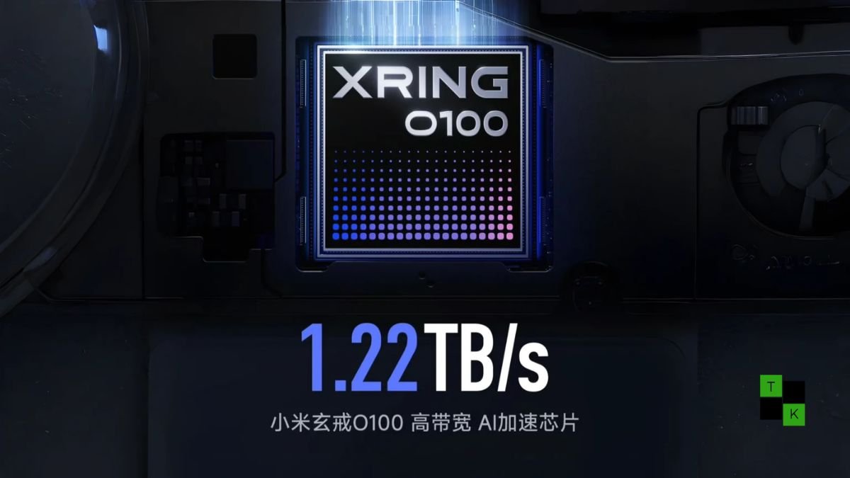
Xiaomi has officially pulled back the curtain on its semiconductor roadmap with the announcement of the Xiaomi Xring O100 (玄戒 O100). Rather than competing as a conventional monolithic mobile System-on-Chip (SoC), the O100 is engineered as a dedicated, high-bandwidth edge AI accelerator designed to solve the physical memory constraints that choke on-device generative AI.
By deploying advanced 3D wafer-level packaging on a mature 6nm process, the accelerator delivers 1.22 TB/s of near-memory bandwidth-roughly 16 times that of mainstream smartphone memory-enabling lightning-fast local large language model (LLM) execution without cloud dependence.
30-Second TL;DR
- Core Purpose: Dedicated edge AI accelerator designed for rapid, private, on-device generative AI inference.
- Packaging Breakthrough: Utilizes Wafer-on-Wafer (WoW) 3D stacking with direct hybrid bonding (1.4 μm pitch, 0.7 μm TSVs) to sandwich two AI-customized DRAM wafers directly atop a 6nm logic die.
- Massive Bandwidth: Reaches 1.22 TB/s near-memory bandwidth, bringing HBM-class data throughput to edge client hardware.
- Real-World Speed: Generates up to 330 tokens per second (TPS) running Xiaomi’s native MiMo 3B parameter model.
- Compute Architecture: Packs a 14-core NPU connected via an adaptive high-bandwidth matrix bus.
- Target Platforms: Destined for the “Xiaomi AI Cube” mini-PC, flagship mobile devices, EVs, and autonomous robotics starting in 2027.
Overcoming the Memory Wall: 3D Wafer-on-Wafer Stacking
Running generative AI and transformer-based neural networks locally requires immense computational horsepower, but the true bottleneck in modern mobile devices is almost always memory bandwidth-often referred to as the “Memory Wall.” Conventional smartphone memory buses (such as LPDDR5X or LPDDR6) operate over planar board traces, capping bandwidth between 68 GB/s and 114 GB/s.
The Xring O100 bypasses horizontal board traces through 3D vertical integration:
- Wafer-on-Wafer (WoW) Hybrid Bonding: Fabricated at TSMC, the chip takes a 6nm logic wafer and bonds two dedicated high-density DRAM wafers directly on top of it.
- Micro-Scale Interconnects: The wafers connect face-to-face using direct copper-to-copper metal hybrid bonding at an ultra-fine 1.4-micron (1.4 μm) bonding pitch.
- Dense Through-Silicon Vias: Vertical communication utilizes 0.7-micron (0.7 μm) TSVs, shortening physical signal travel distances between memory cells and compute logic from millimeters down to fractions of a micrometer.
This physical proximity eliminates parasitic electrical resistance and capacitance, achieving near-memory bandwidth of 1.22 TB/s while maintaining thermal viability on a cost-effective 6nm lithography node.
1.22 TB/s Bandwidth and 330 TPS Local LLM Inference
In local LLM execution, generating text tokens is fundamentally a memory-bound operation. During the auto-regressive decode phase, every newly predicted word requires the chip to reload billions of model weight parameters from memory.
- 330 Tokens Per Second: When executing Xiaomi’s in-house MiMo 3B (3-billion parameter) model, the Xring O100 achieves an inference speed of up to 330 tokens per second.
- Instantaneous Response: At 330 TPS, generation occurs faster than the human eye can read, transforming voice transcription, on-screen translation, and code completion from a delayed query-and-wait loop into an immediate, real-time interaction.
- Data Privacy: Because the throughput is handled entirely within the stacked silicon module, complex reasoning workflows run without uploading user data or biometric prompts to external cloud servers.
14-Core NPU and High-Bandwidth Matrix Bus
Beyond the stacked physical memory, the compute engine of the O100 is engineered around an asymmetric neural architecture:
- 14-Core Dedicated NPU: The computing core features a 14-core neural processing cluster split into specialized compute modules tuned for mixed-precision matrix multiplication (FP16, INT8, and INT4).
- Proprietary Matrix Bus: Xiaomi developed an internal high-bandwidth matrix bus connecting each NPU core directly to the memory stack.
- Dynamic Routing Topology: During LLM processing, the prefill phase (processing the initial prompt prompt context) and the decode phase (generating words sequentially) exhibit drastically different computational profiles. The O100’s matrix bus dynamically alters data routing paths on the fly, shifting resources between high-throughput parallel compute and latency-critical memory streaming.
Xiaomi Xring O100: Architectural Specifications
| Parameter / Feature | Xiaomi Xring O100 (Confirmed Architecture) |
| Chip Classification | Dedicated Edge AI Accelerator (On-Device Inference) |
| Foundry / Process Node | TSMC 6nm Logic Die |
| Packaging Architecture | 3D Wafer-on-Wafer (WoW) Vertical Stacking |
| Memory Configuration | Dual-Layer AI DRAM Wafers Stacked Vertically |
| Bonding Pitch | 1.4 μm Face-to-Face Copper Hybrid Bonding |
| Vertical Interconnect | 0.7 μm Through-Silicon Vias (TSVs) |
| Near-Memory Bandwidth | 1.22 TB/s (HBM-Class Edge Throughput) |
| NPU Compute Cores | 14-Core Asymmetric NPU Cluster |
| Internal Data Bus | Proprietary High-Bandwidth Dynamic Matrix Bus |
| Inference Performance | Up to 330 Tokens/sec (MiMo 3B Parameter Model) |
| Target Launch Horizon | Commercial Mass Production in 2027 |
The Broader XRING Ecosystem and Deployment Roadmap
The Xring O100 is not a standalone experiment; it forms one pillar of Xiaomi’s unified semiconductor strategy:
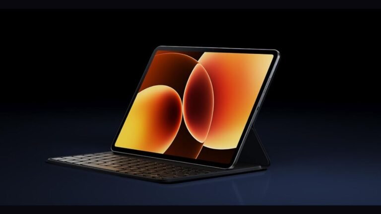
- XRING O3 (Mobile Flagship): The 3nm flagship mobile SoC running inside the Xiaomi 18 Fold and Pad 9 Pro Max.
- XRING D100 (Automotive): A 3nm smart-cockpit and autonomous driving processor packing a 20-core CPU, 16-core NPU, and support for up to 160GB of unified memory to power large models inside Xiaomi Auto vehicles.
- Xiaomi AI Cube & Hardware Prototypes: Xiaomi has already validated working O100 prototypes inside high-performance tablets and compact edge compute appliances termed the Xiaomi AI Cube.
Supported by Xiaomi CEO Lei Jun’s committed CNY 50 billion (~$7 Billion USD) decade-long silicon investment fund, the Xring O100 is scheduled to exit prototype validation and enter commercial mass production across consumer devices and smart robotics in 2027.
🚨 Stay Updated with TopKhoj! 🚨
Get the latest tech news, deals, and exclusive offers first!
📰 Visit News Section📲 Join our Telegram Channel for real-time updates and best deals!
🔗 Join Telegram Now💡 Stay informed and never miss a great deal with TopKhoj!
⚠️ Disclaimer: Any link provided in the article related to a product or service will redirect you to our affiliate partner(s)' website, which are affiliate links. This means that if you make a purchase through these links, we may earn a commission at no extra cost to you. This commission helps support our blog and our work.
🔔 All prices mentioned above are subject to change based on current offers and availability on e-commerce platforms. Please check the latest price and product details on the product page before making a purchase.