Add TOPKHOJ as a Preferred Source on Google
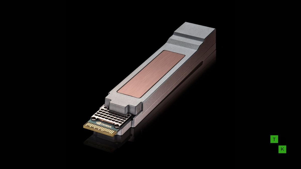
At the Open Compute Project (OCP) Global Summit 2026 in San Jose, NVIDIA and Cisco introduced the Ultra-Dense Small Form Factor Pluggable (USFP)-a next-generation optical transceiver module engineered to expand AI computing clusters without adding network complexity.
Designed as the industry’s first optical interconnect module to support electrical signaling rates of 400Gb/s per lane, USFP enables an aggregate throughput of up to 12.8Tb/s per module. By delivering four times the bandwidth density of existing 200G-per-lane optical interfaces and approximately 1.3 times the energy efficiency, the standard permits hyperscale datacenter operators to attach significantly more compute nodes to individual switches, eliminating the latency penalties, physical footprint, and capital costs associated with building additional switching tiers.
Solving the AI Scale-Up Problem: The Bandwidth Bottleneck
Modern artificial intelligence factories training trillion-parameter foundation models or handling real-time multimodal inference have fundamentally outpaced conventional datacenter networking:
- The Problem with Layered Switching Tiers: In conventional spine-and-leaf network fabrics, once a top-of-rack or aggregation switch runs out of physical port bandwidth, architects must introduce extra intermediate switching layers. Every additional tier multiplies optical transceivers, introduces packet serialization latency, increases synchronization jitter across parallel GPU pipelines, and consumes megawatts of datacenter power.
- Preserving the Pluggable Operating Model: While co-packaged optics (CPO) and proprietary optical engines have been proposed as alternatives, they introduce challenging thermal coupling and require replacing entire switch motherboards when a single laser diode fails. USFP preserves the operational simplicity, field serviceability, and vendor interoperability of traditional front-panel pluggable transceivers while scaling electrical performance.
- Density Multipliers: The first generation of USFP modules packages 16 full-duplex lanes into an enclosure comparable to the standard OSFP footprint, with architectural headroom to scale outward to 32 full-duplex lanes and beyond in subsequent revisions.
Hardware Innovations: 2D Array Connectors and 100W Thermal Handling
Accommodating 400Gb/s across each electrical lane requires addressing signal attenuation and high-temperature dissipation:
- Two-Dimensional Array Connector: USFP incorporates a specialized two-dimensional array interface featuring a two-step insertion design. This configuration distributes mechanical insertion force, dramatically mitigates pin contact wear during field replacements, and preserves high-frequency signal integrity across tight tolerances.
- Passive 100-Watt Thermal Envelope: Traditional optical modules often require auxiliary liquid cold plates or embedded micro-cooling circuits when pushed beyond 40 watts. USFP’s mechanical chassis is engineered to passively dissipate up to 100 watts of thermal load via standard chassis airflow, integrating an oversized copper heat-spreading plate and chassis finning.
- Switch and SuperNIC Interoperability: The module footprint is designed to seat cleanly in both multi-terabit Ethernet spine switches and host-side SuperNICs and SmartNICs mounted inside GPU server blades, creating a unified end-to-end optical fabric.
Optical Transceiver Evolution: USFP vs. Prior Generations
| Architectural Specification | Current 100G Optics (QSFP-DD) | Current 200G Optics (OSFP) | Next-Gen USFP (NVIDIA & Cisco) |
| Electrical Signaling Per Lane | 100Gb/s PAM4 | 200Gb/s PAM4 | 400Gb/s PAM4 / Next-Gen Signaling |
| Active Lane Architecture | 8 Full-Duplex Lanes | 8 Full-Duplex Lanes | 16 Full-Duplex Lanes (Scalable to 32+) |
| Aggregate Module Capacity | 800Gb/s (0.8Tb/s) | 1.6Tb/s | Up to 12.8Tb/s Per Module |
| Bandwidth Density Factor | 1x Baseline | 2x Baseline | 4x Density vs. 200G Optics |
| Relative Power Efficiency | Baseline | ~1.0x | ~1.3x More Efficient (Less Power/Bit) |
| Thermal Dissipation Limit | Up to 20W – 25W | Up to 35W – 40W | Up to 100W Continuous Dissipation |
| Insertion Mechanism | Single-Step Friction Edge | Standard Card Edge | Two-Dimensional 2-Step Insertion |
| Target Infrastructure Tier | Cloud Webscale / 100G Leaf | AI Clusters (H100/H200) | Next-Gen Multi-Gigawatt AI Factories |
Building an Open Multi-Source Ecosystem: TE and Amphenol Partnerships
Rather than locking the technology behind a walled garden, NVIDIA and Cisco are establishing an open hardware standard:
- Multi-Source Agreement (MSA) Foundation: NVIDIA and Cisco confirmed they are actively collaborating with tier-one interconnect manufacturers TE Connectivity and Amphenol to develop standardized USFP connector cages, electrical pins, and passive thermal enclosures.
- Community-Led Open Specification: Both firms plan to submit the complete USFP mechanical, electrical, and thermal guidelines to an upcoming open community project-enabling third-party optical transceiver vendors to produce compliant modules.
- Ecosystem-Wide Adoption: By establishing broad supplier sourcing, datacenter operators can source transceivers from competitive global suppliers without single-vendor lock-in, accelerating the transition to 400G-per-lane networks across global telecom and cloud providers.
Executive Perspectives from OCP 2026
During the announcement in San Jose, technical leadership emphasized the holistic role interconnects play in scaling compute fabrics:
- NVIDIA’s Perspective: NVIDIA leadership noted that scaling the next generation of generative AI datacenters begins by re-engineering the smallest physical connections. Developing USFP enables operators to expand cluster boundaries efficiently while keeping networking power from consuming an unsustainable share of total datacenter capacity.
- Cisco’s Full-Stack View: Cisco executives emphasized that reaching 400Gb/s per lane required moving beyond incremental tweaks to legacy form factors. By taking a unified approach across silicon, switching hardware, physical optics, and network software, the collaboration delivers higher density while retaining field serviceability and operational simplicity.
Implementation Roadmap and Availability
The transition to USFP-based optical infrastructure will roll out alongside next-generation network hardware:
- Interconnect Availability: Sampling of USFP passive cages, test boards, and physical connector assemblies from TE Connectivity and Amphenol will commence through early 2027.
- Commercial Hardware Deployment: First-generation commercial switches, SuperNICs, and transceivers adopting the USFP standard are scheduled for volume datacenter shipments starting in late 2027, coinciding with broader commercial rollouts of next-generation AI accelerators.
By quad-doubling front-panel bandwidth density and boosting energy efficiency across every bit transmitted, NVIDIA and Cisco’s USFP standard provides a practical, serviceable pathway for scaling multi-gigawatt AI computing environments.
🚨 Stay Updated with TopKhoj! 🚨
Get the latest tech news, deals, and exclusive offers first!
📰 Visit News Section📲 Join our Telegram Channel for real-time updates and best deals!
🔗 Join Telegram Now💡 Stay informed and never miss a great deal with TopKhoj!
⚠️ Disclaimer: Any link provided in the article related to a product or service will redirect you to our affiliate partner(s)' website, which are affiliate links. This means that if you make a purchase through these links, we may earn a commission at no extra cost to you. This commission helps support our blog and our work.
🔔 All prices mentioned above are subject to change based on current offers and availability on e-commerce platforms. Please check the latest price and product details on the product page before making a purchase.